|
Introduction |
|
|
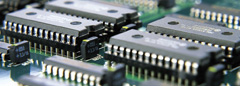
Multilayer PCB's represent one of the most complicated products in the PCB industry. A breakdown of a multilayer PCB shows that it consists of three basic elements: thin rigid laminates, prepreg sheet for bonding the laminates and copper foils. |
|
|
|
|
Purpose of Multilayer PCBs |
|
|
* To accommodate a larger number of interconnections that steadily increasing use of high pin-count integrated circuits(IC). |
|
* To establish an electrical performance of the multilayer PCB, such as voltage and ground planes, EMC-shielding and circuit speed etc. |
|
|
|
|
Material |
|
|
Thin laminate and Copper foil |
|
|
Vendor |
Model |
Thickness |
Copper |
TG |
ER |
SHENGYI |
S1141 |
0.05-3.2 mm |
17-105 μm |
≥130 |
≤5.4 |
SHENGYI |
S1170 |
0.05-3.2 mm |
17-105 μm |
≥170 |
≤5.4 |
ITEQ |
IT-140 |
0.05-1.5 mm |
17-175 μm |
>135 |
<5.4 |
ITEQ |
IT-180 |
0.05-1.5 mm |
17-175 μm |
>170 |
<5.4 |
ITEQ |
IT-180A |
0.05-1.5 mm |
17-175 μm |
>170 |
<5.4 |
|
|
|
|
|
|
Prepreg |
|
|
Type of Prepreg |
Pressed Thickness |
Resin Content |
|
mm |
mil |
% |
7628H(7630) |
0.213 |
8.4 |
50 |
7628(43%) |
0.195 |
7.6 |
43 |
7628(41%) |
0.185 |
7.3 |
41 |
2116HR |
0.135 |
5.3 |
57 |
2116 |
0.120 |
4.7 |
52 |
2113 |
0.100 |
4.0 |
56 |
1080 |
0.076 |
3.0 |
64 |
1060 |
0.050 |
2.0 |
71 |
|
|
|
|
|
|
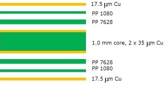
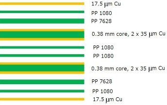
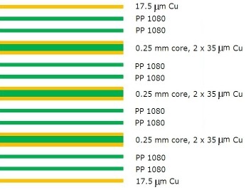
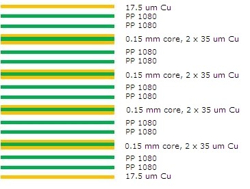
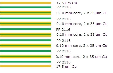
Stack up |
|
|
The purpose of stack-up is to interleave the thin laminates and the prepreg sheets in correct sequence and ensure correct layer-to-layer registration. |
|
The stack-up of multilayer boards can be done in many different ways. The choice is often determined by the types of thin laminate and prepreg sheet we have in the stock. Unless there are special demands for the controlled impdedances, it is normally most cost-effective to let us choose the stack-up list shown below. |
|
|
|
|
|
|
|
|
|
|
|
|
|
|
|
|
|
|
|
|
|
|
|
|
|
|
|
|
|
|
|
|
|
|
|
|
|
|
|
|
|
|
|
|
|
|
|
|
|
|
|
|
|
|
|
|
|
|
|
|